|
|
|
About this capture | ||||||||||||||
|
|
|
About this capture | ||||||||||||||
What is this?
The problem
The solution
How I did it
Tying it all together
Circuit operation
Updates / feedback
This page describes a modification to a Sinclair ZX Spectrum 48K: replacement of the lower 16K RAM with a single SRAM chip. The circuit may also work in other places where 4116 type DRAMs (16K x 1) are used. However: that has NOT been tested! This page is not a "how to", but a "how it was done". Anything shown here may or may not work for you, and I am not responsible if you destroy your own equipment!
It also applies to the ZX Spectrum+, since that model uses the same motherboard as a Spectrum 48K. It does not apply to Spectrum 128K or Amstrad models, since they don't use 4116 type DRAMs.
The ZX Spectrum 16/48K models have RAM memory divided in 2 banks:
This use of 4116 type DRAMs is problematic for several reasons:
... is a generic one: don't replace the part(s), but replace the function of the part(s). In this case: a 16K x 8 bit RAM, with multiplexed address inputs, timing requirements that match those of a 4116 DRAM, a single +5V supply, a pinout that easily fits a ZX Spectrum circuit board, is cheap and can be bought around the corner.
Unfortunately, I don't know of any such thing. So the next best option: find or create something that is 'close enough'. I opted to try and get a 32K x 8 bit SRAM to take the 4116 DRAM's place (using only half of the SRAM's 32K), and find a way to route control signals such that normal operation would occur. I prefer SRAM over DRAM for this application because:
Main difference between SRAMs and DRAMs is that DRAMs normally use multiplexed address inputs: part of the address is placed on these inputs, activation of the /RAS signal causes the DRAM to 'remember' their value internally, and a subsequent activation of the /CAS signal informs the DRAM that its inputs now carry the remaining address bits. On the other hand, an SRAM reads all address signals at once (with the drawback that more IC pins are used). Another difference is that 4116 DRAMs have separate data inputs and outputs. This is not a problem though: in most places where 4116 type IC's are used (ZX Spectrum included), you will see that data inputs and outputs are connected, and form a signal which is read by one pin (2), and used as output by another pin (14).
Click to view relevant section of ZX Spectrum schematic (issue 4A/B):

Initial idea was to use a register to capture these address bits (as a DRAM would), feed its output to half the SRAM address inputs, and connect the other half of SRAM address inputs to the multiplexed address lines directly. The /RAS signal would clock the register, and other DRAM control signals would be connected to SRAM control inputs (without additional logic, if possible!). This worked, but not 100%: Z80 operation was perfectly stable, but screen output got corrupted sometimes. This would show as short lines of discolored pixels (color data garbled, mostly in loading screens). I tried delaying the /RAS signal with an RC combo. This improved operation somewhat, but with too high RC time the Spectrum would lock up. Then I tried additional logic between the other SRAM control signals, this didn't help at all... Back to the drawing board!
 (click for larger version)
I realized that these DRAMs capture half of the address at the falling edge (high-to-low transition) of the /RAS signal, and did what I had rather avoided: add more logic. A simple inverter, but still an extra IC (74HC04, lower left corner in picture below). This did give the desired effect: Z80 operation, stability and screen output were all fine. After testing a bunch of software I felt confident enough to construct a more permanent solution than the wire mess I had so far. A digital diary that had been sitting unused in a box for years (and highlighted "32K" on the package) had a physically smaller, but suitable SRAM type inside. So I used that to construct something that would fit on the Spectrum circuit board, and allow the case (rubber key model) to be closed.

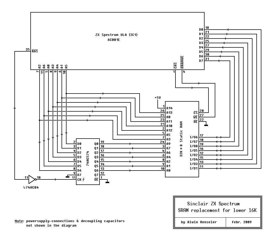
I checked this schematic thoroughly against my modded Speccy, after drawing it. Exact pins used don't matter for a number of signals, but the schematic shows exactly how things are wired up in my 'prototype'. Please note the following:
Some things may happen to DRAMs under normal operation, that is not relevant for an SRAM:
As you can see, the SRAM's /OE (Output Enable) is grounded, read: always on. This doesn't mean the SRAM always tries to output data: the simplest way of looking at it, is to think that /CS (Chip Select) must be activated for the SRAM to do anything at all, and with /CS active, the /WE (Write Enable) decides if data is read (=output for the SRAM), or written (=input for the SRAM). In case of doubt: check the SRAM's datasheet to see how it works exactly.
I suspect that any ordinary 32K x 8 bit static RAM, with access times in the range of, say, 70~150 ns. would work similarly as the parts I used. SRAMs of this type can be found in many places (and devices!), and I'm not going to bother listing possible sources. One word of warning though: whatever you'd like to use, make sure to get a datasheet for the part you have, verify its pinout, supply voltage, logical function and (if you're feeling brave) timing diagrams. Not all SRAMs are created equal! Also I would avoid high speed cache SRAMs: their fast response may be fine, but they will also switch their outputs much faster (short rise & fall times), and that can cause problems in any circuit that wasn't designed for it - like the ZX Spectrum.
The register used is a 74HC574. This register is clocked at the rising edge (low-to-high transition) of its clock input. The inverter causes that to match the falling edge (high-to-low transition) of the /RAS signal. I think this is a crucial aspect of what makes the circuit work: after clocking in the address bits, the address inputs may change, the /RAS signal can go inactive, but the register outputs will remain unchanged until the next falling edge of /RAS. This in contrast to other register types (for example: 74LS373), that allow their outputs to follow inputs as long as its clock / latch enable signal is held at a specific logic level. This may work fine, but it must be understood that circuit operation is different if such register type is used.
A register that is clocked on the falling edge (high-to-low transition) of its clock input, would be nice: that would do away with the inverter, simplify the circuit, and perhaps make it faster. If you know a suitable type: please let me know!
As for logic family: I used 74HCxxx parts because they had the required logical function, I have used 74HC parts successfully in similar circuits, and this is what I had laying around ;-) 74HCT and 74LS types should work the same here. I suspect faster logic like 74AC(T) would be fine, but this would influence timing, and therefore needs testing.
Right now, this circuit could use a lot more testing: on different issue Spectrum boards, with different version ULA's, using different logic IC / logic families, SRAMs, construction methods and test software. It is my hope that it will turn into a generic, easy to use, easy to obtain, low-power, reliable replacement for 4116 DRAMs, wherever these are found: ZX Spectrums, other homecomputers, as video memory for TMS9918 chips, arcade machines, etc, etc. I don't know if that will be possible. I have just a few machines available for testing, and I don't plan to do all the work. That's where you come in: if you try this circuit (or a variation of it) somewhere, please let me know how it works, even if it doesn't! The more datapoints, the easier it becomes to determine what works & what doesn't, and the faster we might have something that works 'everywhere'. Some updates:
If you want to replace a single 4116 DRAM, it may be easier to try and use a 64K x 1 DRAM (4164 or equivalent type) as replacement. See here for details. Haven't tried this myself, since my goal was to replace the whole set of 4116 DRAMs, use parts than can be obtained new, remove dependency on +12V and -5V, and reduce power consumption. Using 64K x 1 DRAMs meets some, but not all these goals. Somebody even used a SIMM as lower RAM replacement - me thinks a 32K x 8 SRAM + some logic is a better option.
With the 4116 DRAMs gone, you don't need the -5V supply voltage anymore - it isn't used anywhere else. The +12V supply voltage is still used in the video encoding circuitry. I have verified that it's possible to replace the video circuitry's +12V supply with the unregulated DC input voltage (that goes into the 7805 regulator). Around 10~15V works fine, without visible side-effects. This 10~15V range is probably wider, but you may run into other issues when you exceed it (power consumption of individual parts, for one).
You might need to be more careful in selecting the external power supply for your ZX Spectrum (original power supply = OK). However: with 4116 DRAMs gone and video power supply re-routed, all onboard voltage conversion circuitry isn't needed anymore. The ~12V AC it produces, goes to the edge connector. Meaning: you may have problems with some peripherals when missing. If the peripherals you use with your Spectrum don't use this AC voltage (or you don't use any peripherals with that ZX Spectrum), it's safe to disable or even remove the voltage conversion circuitry. Normally there's little reason to do so, but it may eliminate some failure modes, and reduces component count quite a bit. Also you could re-route the +12V video power supply to reduce the load on the voltage conversion circuitry, but leave this circuitry in place.
On issue 2 and issue 3A/B boards, several gates of IC24 (74LS00, sometimes 74HCT00) are not used. Connect one of these unused inputs to +5V, and the other input (+corresponding output) works as inverter, so that you don't have to add one. Issue 1 boards don't include support for the upper 32K RAM (an add-on board might be used, and besides: the rare issue 1's are more valuable to collectors in original state). Issue 4A/B boards use these gates as a timing delay between ULA and IC3/IC4 address multiplexers (74LS157), later issue boards replace this logic with a custom IC.
If you use these gates: don't blindly trust the schematic (check the board itself), and make sure the pins aren't connected to anything else! For example by cutting them loose from the board.
There exist IC's that include just a single logic gate. Such an IC type would be smaller (usually SMD), but might be harder to find. Also it's possible to use a transistor as inverter. I don't recommend this for several reasons, but others may disagree.
Richard Gellman ("splodge" at the site "starfleet-net.co.uk") writes: "Thought you might like to know, its been used successfully on a Memotech MTX 512 as a replacement for the main RAM. The only caveat is that the wires on LK6 need to be set horizontal and EAST. By default they are set WEST, which prevents the mod from working. LK6 is reminiscent of the RAS or CAS delay selector on the later ZX Spectrums (used to delay either RAS or CAS to suit DRAM timings). The parts used were a 74HC574, 74F04 and AS7C512-15 64kx8 SRAM. All surface mount parts."
There's probably an easier way to use SRAM for MTX512 main memory, but apparently the MTX512 schematic is Missing In Action ??
4116 DRAMs were often used as video RAM connected to a TMS9918 (or related type) videochip. This thread on the MSX.org forum made it clear that you can't use this circuit for TMS9918 video RAM. The TMS9918 sends address and VRAM write data over the same lines, reads VRAM data over another set of lines (using the 4116 separate 'Q' outputs), and uses some 'non-obvious' signal timing to make this work. An SRAM as video RAM is surely possible, but would likely require an address- and data latch. And it's unclear at this point how to arrange / control these latches. To be continued..?